

In the past schematic drawings and PCB layouts were meticulousyhand-crafted, and those skliledin these arts were highly sought after. However, in todays age, ECAD tols have revolutionized the creation of these PCB diagrams. Transitioning from a schematic to a PCB layout has become an automated process facilitated by comnputer software.

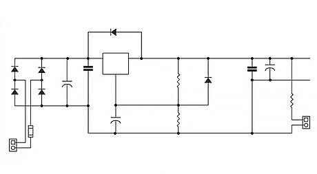
Routing and tracing entall wiring atask often considered the most pCB layout. This complexity intensifes in the case of multilayer boards with a significant number of vertical through-holes (PTH) that trensmit signals; internally and- to the ground plane. Adhering tO proper spacing and gap.regulations during.track routingiscrucial

Efficiently organizing components is the next pivotal step. Post partitioning and adhering to licensing rules, position the components on the board. This meticulous arrangement is fundamental to the successful construction of the board.

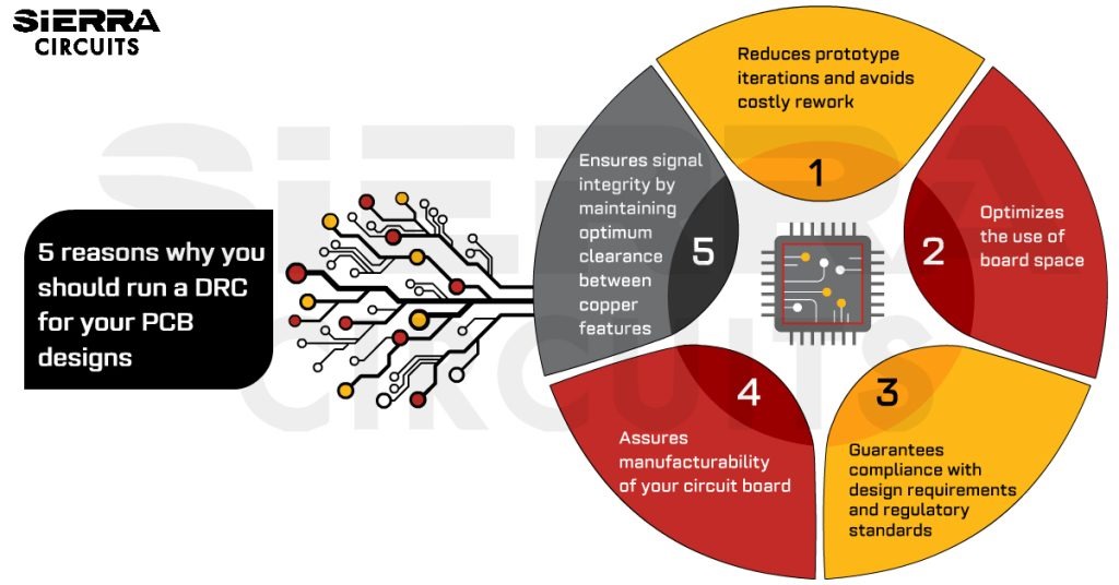
Before finalizing the PCB design, it's essential to perform meticulous checks for- any errors. Integrate a Design Rule Check/(DRC) assessment to verify if your design aligns with the prescribed layout guidelines and restrictions. These regulations should align with the CM's Design for Manufacturabilty (DFM) guidelines to ensure manufacturability.
After defining the board size, materials,layercount, and type, proceed to establish the stack confguration. This foundational step lays the groundwork for the subsequent design process.
Commence thep process selecting the appropriate dimensions for the circuit board. While most ECAD tools offer preset board sizes and customizable options for area and thickness.
Design for Manufacturability (DFM) is an essential part of the PCB fabrication process. Since manufacturing involves many steps, DFM helps ensure the design translates smoothly into production without issues that lead to defects or delays.
Our engineers analyze layouts upfront to confirm they meet the capabilities of Highleap’s advanced fabrication equipment and materials. DFM allows optimizing boards for our tight machining tolerances and precision processes.
Here are the key advantages of implementing DFM in PCB design and manufacturing:
DFM minimizes the need for design modifications to accommodate manufacturing processes, reducing the risk of compromising product quality. By aligning the design with manufacturing capabilities, DFM helps deliver PCBs with fewer defects and higher overall quality.
DFM ensures that PCB designs align with the capabilities and tolerances of PCB manufacturing machines and materials. This alignment minimizes discrepancies between the intended design and the manufacturable product, streamlining the production process.
DFM empowers PCB designers to create boards optimized for efficient large-scale production. Lower costs stem from a reduced number of errors identified during the manufacturing process. By minimizing the need for design modifications and rework, DFM contributes to cost-effective PCB production.
The PCB manufacturing process involves multiple stages, each susceptible to potential errors. DFM mitigates delays caused by defective products, errors, and extensive project review and documentation checks. This accelerates time to market, a critical factor in competitive industries.
DFM considers critical parameters like annular ring size, vital for maintaining electrical connections in PCBs. Highleap highlights the importance of designing annular rings with adequate width to accommodate slight misalignments between layers in multilayer PCBs, ensuring reliable electrical connections.
Aggressive advanced fabrication equipment and precise processes demand designs tailored to tight machining tolerances. DFM is instrumental in optimizing PCB layouts to meet these rigorous standards, ensuring high-quality, error-free manufacturing and seamless integration with Highleap’s cutting-edge capabilities.
Aggressive - Copyright 2025. All rights reserved.